W25Q256FV
3V 256M-BIT
SERIAL FLASH MEMORY WITH
DUAL/QUAD SPI & QPI
Publication Release Date: February 26, 2016
Preliminary
Revision I
�W25Q256FV
Table of Contents
1.
GENERAL DESCRIPTIONS ............................................................................................................. 5
2.
FEATURES ....................................................................................................................................... 5
3.
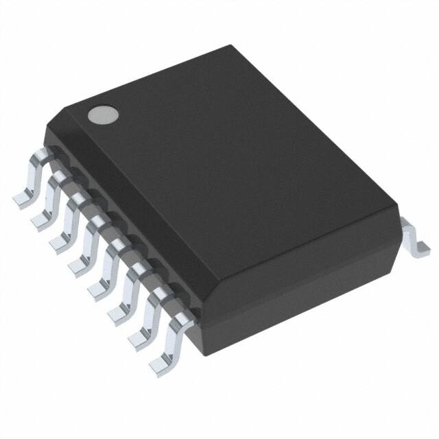
PACKAGE TYPES AND PIN CONFIGURATIONS........................................................................... 6
4.
3.1
Pad Configuration WSON 8x6-mm ...................................................................................... 6
3.2
Pad Description WSON 8x6-mm .......................................................................................... 6
3.3
Pin Configuration SOIC 300-mil ........................................................................................... 7
3.4
Pin Description SOIC 300-mil ............................................................................................... 7
3.5
Pin Configuration PDIP 300-mil ............................................................................................ 8
3.6
Pin Description SOIC 150/208-mil, WSON 6x5-mm / USON 4x3-mm / PDIP 300-mil ........ 8
3.7
Ball Configuration TFBGA 8x6-mm (5x5 or 6x4 Ball Array) ................................................. 9
3.8
Ball Description TFBGA 8x6-mm ......................................................................................... 9
PIN DESCRIPTIONS ...................................................................................................................... 10
4.1
Chip Select (/CS) ................................................................................................................ 10
4.2
Serial Data Input, Output and IOs (DI, DO and IO0, IO1, IO2, IO3) ................................... 10
4.3
Write Protect (/WP) ............................................................................................................ 10
4.4
HOLD (/HOLD) ................................................................................................................... 10
4.5
Serial Clock (CLK) .............................................................................................................. 10
4.6
Reset (/RESET) .................................................................................................................. 10
5.
BLOCK DIAGRAM .......................................................................................................................... 11
6.
FUNCTIONAL DESCRIPTIONS ..................................................................................................... 12
6.1
6.2
7.
SPI / QPI Operations .......................................................................................................... 12
6.1.1
Standard SPI Instructions ..................................................................................................... 12
6.1.2
Dual SPI Instructions ............................................................................................................ 12
6.1.3
Quad SPI Instructions ........................................................................................................... 13
6.1.4
QPI Instructions .................................................................................................................... 13
6.1.5
3-Byte / 4-Byte Address Modes ............................................................................................ 13
6.1.6
Hold Function ....................................................................................................................... 14
6.1.7
Software Reset & Hardware /RESET pin .............................................................................. 14
Write Protection .................................................................................................................. 15
STATUS AND CONFIGURATION REGISTERS ............................................................................ 16
7.1
Status Registers ................................................................................................................. 16
7.1.1
Erase/Write In Progress (BUSY) – Status Only ................................................................ 16
7.1.2
Write Enable Latch (WEL) – Status Only .......................................................................... 16
7.1.3
Block Protect Bits (BP3, BP2, BP1, BP0) – Volatile/Non-Volatile Writable ....................... 17
7.1.4
Top/Bottom Block Protect (TB) – Volatile/Non-Volatile Writable ....................................... 17
7.1.5
Complement Protect (CMP) – Volatile/Non-Volatile Writable ............................................ 17
-1-
�W25Q256FV
7.2
8.
7.1.6
Status Register Protect (SRP1, SRP0) – Volatile/Non-Volatile Writable ........................... 17
7.1.7
Erase/Program Suspend Status (SUS) – Status Only....................................................... 18
7.1.8
Security Register Lock Bits (LB3, LB2, LB1) – Volatile/Non-Volatile OTP Writable .......... 18
7.1.9
Quad Enable (QE) – Volatile/Non-Volatile Writable .......................................................... 18
7.1.10
Current Address Mode (ADS) – Status Only ................................................................... 19
7.1.11
Power-Up Address Mode (ADP) – Non-Volatile Writable ................................................ 19
7.1.12
Write Protect Selection (WPS) – Volatile/Non-Volatile Writable ..................................... 19
7.1.13
Output Driver Strength (DRV1, DRV0) – Volatile/Non-Volatile Writable ......................... 20
7.1.14
/HOLD or /RESET Pin Function (HOLD/RST) – Volatile/Non-Volatile Writable .............. 20
7.1.15
Reserved Bits – Non Functional ...................................................................................... 20
7.1.16
W25Q256FV Status Register Memory Protection (WPS = 0, CMP = 0) ............................ 21
7.1.17
W25Q256FV Status Register Memory Protection (WPS = 0, CMP = 1) ............................ 22
7.1.18
W25Q256FV Individual Block Memory Protection (WPS=1) .............................................. 23
Extended Address Register – Volatile Writable Only ...................................................... 24
INSTRUCTIONS ............................................................................................................................. 25
8.1
8.2
Device ID and Instruction Set Tables ................................................................................. 25
8.1.1
Manufacturer and Device Identification ................................................................................ 25
8.1.2
Instruction Set Table 1 (Standard/Dual/Quad SPI, 3-Byte & 4-Byte Address Mode)(1) ......... 26
8.1.3
Instruction Set Table 2 (Standard/Dual/Quad SPI Instructions, 3-Byte Address Mode)(1) .... 27
8.1.4
Instruction Set Table 3 (Standard/Dual/Quad SPI Instructions, 4-Byte Address Mode)(1) .... 28
8.1.5
Instruction Set Table 4 (QPI Instructions, 3-Byte & 4-Byte Address Mode)(14) ..................... 29
8.1.6
Instruction Set Table 5 (QPI Instructions, 3-Byte Address Mode)(14) .................................... 30
8.1.7
Instruction Set Table 6 (QPI Instructions, 4-Byte Address Mode)(14) .................................... 30
Instruction Descriptions ...................................................................................................... 32
8.2.1
Write Enable (06h) ............................................................................................................... 32
8.2.2
Write Enable for Volatile Status Register (50h) .................................................................... 32
8.2.3
Write Disable (04h) ............................................................................................................... 33
8.2.4
Read Status Register-1 (05h), Status Register-2 (35h) & Status Register-3 (15h) .............. 33
8.2.5
Write Status Register-1 (01h), Status Register-2 (31h) & Status Register-3 (11h) .............. 34
8.2.6
Read Extended Address Register (C8h) .............................................................................. 37
8.2.7
Write Extended Address Register (C5h) .............................................................................. 38
8.2.8
Enter 4-Byte Address Mode (B7h) ........................................................................................ 39
8.2.9
Exit 4-Byte Address Mode (E9h) .......................................................................................... 39
8.2.10
Read Data (03h) ................................................................................................................. 40
8.2.11
Read Data with 4-Byte Address (13h) ................................................................................ 41
8.2.12
Fast Read (0Bh) ................................................................................................................. 42
8.2.13
Fast Read with 4-Byte Address (0Ch) ................................................................................ 44
8.2.14
Fast Read Dual Output (3Bh) ............................................................................................. 45
8.2.15
Fast Read Dual Output with 4-Byte Address (3Ch) ............................................................ 46
8.2.16
Fast Read Quad Output (6Bh) ............................................................................................ 47
8.2.17
Fast Read Quad Output with 4-Byte Address (6Ch) ........................................................... 48
-2-
Publication Release Date: February 26, 2016
Preliminary –Revision I
�W25Q256FV
9.
8.2.18
Fast Read Dual I/O (BBh) ................................................................................................... 49
8.2.19
Fast Read Dual I/O with 4-Byte Address (BCh) .................................................................. 51
8.2.20
Fast Read Quad I/O (EBh) ................................................................................................. 53
8.2.21
Fast Read Quad I/O with 4-Byte Address (ECh) ................................................................ 56
8.2.22
Word Read Quad I/O (E7h) ................................................................................................ 58
8.2.23
Octal Word Read Quad I/O (E3h) ....................................................................................... 60
8.2.24
Set Burst with Wrap (77h) .................................................................................................. 62
8.2.25
Page Program (02h) ........................................................................................................... 63
8.2.26
Quad Input Page Program (32h) ........................................................................................ 65
8.2.27
Sector Erase (20h) ............................................................................................................. 66
8.2.28
32KB Block Erase (52h) ..................................................................................................... 67
8.2.29
64KB Block Erase (D8h) ..................................................................................................... 68
8.2.30
Chip Erase (C7h / 60h) ....................................................................................................... 69
8.2.31
Erase / Program Suspend (75h) ......................................................................................... 70
8.2.32
Erase / Program Resume (7Ah) ......................................................................................... 72
8.2.33
Power-down (B9h) .............................................................................................................. 73
8.2.34
Release Power-down / Device ID (ABh) ............................................................................. 74
8.2.35
Read Manufacturer / Device ID (90h) ................................................................................. 76
8.2.36
Read Manufacturer / Device ID Dual I/O (92h) ................................................................... 77
8.2.37
Read Manufacturer / Device ID Quad I/O (94h) ................................................................. 78
8.2.38
Read Unique ID Number (4Bh)........................................................................................... 79
8.2.39
Read JEDEC ID (9Fh) ........................................................................................................ 80
8.2.40
Read SFDP Register (5Ah) ................................................................................................ 81
8.2.41
Erase Security Registers (44h) ........................................................................................... 82
8.2.42
Program Security Registers (42h) ...................................................................................... 83
8.2.43
Read Security Registers (48h) ........................................................................................... 84
8.2.44
Set Read Parameters (C0h) ............................................................................................... 85
8.2.45
Burst Read with Wrap (0Ch)............................................................................................... 86
8.2.46
Enter QPI Mode (38h)......................................................................................................... 87
8.2.47
Exit QPI Mode (FFh) ........................................................................................................... 88
8.2.48
Individual Block/Sector Lock (36h) ..................................................................................... 89
8.2.49
Individual Block/Sector Unlock (39h) .................................................................................. 90
8.2.50
Read Block/Sector Lock (3Dh) ........................................................................................... 91
8.2.51
Global Block/Sector Lock (7Eh) .......................................................................................... 92
8.2.52
Global Block/Sector Unlock (98h) ....................................................................................... 92
8.2.53
Enable Reset (66h) and Reset Device (99h) ...................................................................... 93
ELECTRICAL CHARACTERISTICS ............................................................................................... 94
9.1
Absolute Maximum Ratings (1)(2) ...................................................................................... 94
9.2
9.3
9.4
9.5
Operating Ranges............................................................................................................... 94
Power-up Timing and Write Inhibit Threshold(1) ................................................................ 95
DC Electrical Characteristics .............................................................................................. 96
AC Measurement Conditions(1) ......................................................................................... 97
-3-
�W25Q256FV
10.
11.
9.6
AC Electrical Characteristics(6) ........................................................................................... 98
9.7
Serial Output Timing ......................................................................................................... 100
9.8
Serial Input Timing ............................................................................................................ 100
9.9
/HOLD Timing ................................................................................................................... 100
9.10
/WP Timing ....................................................................................................................... 100
PACKAGE SPECIFICATIONS ...................................................................................................... 101
10.1
8-Pad WSON 8x6-mm (Package Code E) ....................................................................... 101
10.2
8-Pin PDIP 300-mil (Package Code A) ............................................................................. 102
10.3
16-Pin SOIC 300-mil (Package Code F) .......................................................................... 103
10.4
24-Ball TFBGA 8x6-mm (Package Code B, 5x5-1 Ball Array) ......................................... 104
10.5
24-Ball TFBGA 8x6-mm (Package Code C, 6x4 Ball Array) ............................................ 105
ORDERING INFORMATION ........................................................................................................ 106
11.1
12.
Valid Part Numbers and Top Side Marking ...................................................................... 107
REVISION IISTORY.................................................................................................................... 108
-4-
Publication Release Date: February 26, 2016
Preliminary –Revision I
�W25Q256FV
1. GENERAL DESCRIPTIONS
The W25Q256FV (256M-bit) Serial Flash memory provides a storage solution for systems with limited
space, pins and power. The 25Q series offers flexibility and performance well beyond ordinary Serial Flash
devices. They are ideal for code shadowing to RAM, executing code directly from Dual/Quad SPI (XIP)
and storing voice, text and data. The device operates on a single 2.7V to 3.6V power supply with current
consumption as low as 4mA active and 1µA for power-down. All devices are offered in space-saving
packages.
The W25Q256FV array is organized into 131,072 programmable pages of 256-bytes each. Up to 256
bytes can be programmed at a time. Pages can be erased in groups of 16 (4KB sector erase), groups of
128 (32KB block erase), groups of 256 (64KB block erase) or the entire chip (chip erase). The
W25Q256FV has 8,192 erasable sectors and 512 erasable blocks respectively. The small 4KB sectors
allow for greater flexibility in applications that require data and parameter storage. (See Figure 2.)
The W25Q256FV support the standard Serial Peripheral Interface (SPI), Dual/Quad I/O SPI as well as 2clocks instruction cycle Quad Peripheral Interface (QPI): Serial Clock, Chip Select, Serial Data I/O0 (DI),
I/O1 (DO), I/O2 (/WP), and I/O3 (/HOLD). SPI clock frequencies of up to 104MHz are supported allowing
equivalent clock rates of 208MHz (104MHz x 2) for Dual I/O and 416MHz (104MHz x 4) for Quad I/O when
using the Fast Read Dual/Quad I/O instructions. These transfer rates can outperform standard
Asynchronous 8 and 16-bit Parallel Flash memories. The Continuous Read Mode allows for efficient
memory access with as few as 8-clocks of instruction-overhead to read a 24-bit address, allowing true XIP
(execute in place) operation.
A Hold pin, Write Protect pin and programmable write protection, with top or bottom array control, provide
further control flexibility. Additionally, the device supports JEDEC standard manufacturer and device ID
and SFDP Register, a 64-bit Unique Serial Number and three 256-bytes Security Registers.
2. FEATURES
New Family of SpiFlash Memories
– W25Q256FV: 256M-bit / 32M-byte
– Standard SPI: CLK, /CS, DI, DO, /WP, /Hold
– Dual SPI: CLK, /CS, IO0, IO1, /WP, /Hold
– Quad SPI: CLK, /CS, IO0, IO1, IO2, IO3
– 3 or 4-Byte Addressing Mode
– Software & Hardware Reset
Highest Performance Serial Flash
– 104MHz Standard/Dual/Quad SPI clocks
– 208/416MHz equivalent Dual/Quad SPI
– 50MB/S continuous data transfer rate
– More than 100,000 erase/program cycles
– More than 20-year data retention
Efficient “Continuous Read”
– Continuous Read with 8/16/32/64-Byte Wrap
– As few as 8 clocks to address memory
– Quad Peripheral Interface (QPI) reduces
instruction overhead
– Allows true XIP (execute in place) operation
– Outperforms X16 Parallel Flash
Low Power, Wide Temperature Range
– Single 2.7 to 3.6V supply
– 4mA active current,